Associate Professor John Cumings
Knowing temperature at the nanoscale (<100nm resolution) is a major challenge for both science and technology. Department of Materials Science and Engineering Professor John Cumings' group, in work published recently in the Journal of Nano Letters and performed in collaboration with Professor David Goldhaber-Gordon at Stanford University, have invented a method to do so using a transmission electron microscope (TEM) and melting transitions in nanoscale metal islands. With the islands acting as distributed, local, passive thermometers, the TEM can be used to map absolute temperature over the entire field-of-view. The technique works in both active and passive devices, and is naturally tailored to measurements on nanowires, nanotubes, and other nanoscale materials.
Traditionally, thermal microscopy is performed by detecting infrared radiation with far-field optics, where resolution is limited by wavelength. Using electrons, smaller wavelengths and higher resolution are possible. An additional obstacle in nanoscale thermometry is accounting for the effect of the probe on the system. Probe-system equilibrium, a necessary condition for temperature to be well-defined, is thus a further requirement along with high resolution. Here, small metal islands are ideally suited to meet this requirement because they combine a small probe size (the diameter of the island) with an intrinsically equilibrium phenomenon (liquid/solid transition).
First, metal islands are deposited on one side of an electron-transparent silicon nitride membrane, loaded into a stage that allows heating inside the microscope, and inserted in the TEM. To image the liquid/solid phase transition, the TEM is used in dark-field mode such that liquid islands appear bright, while solid islands appear dark. This is seen in Figure 1 (scale bar = 1µm), where a) shows the bright field image of indium islands while parts b) and c) show the dark field image for the solid and liquid islands, respectively. This contrast is produced by careful positioning of the objective aperture at the point between the sharp solid ring and the diffuse liquid one, represented by the white circle in Fig. 1b.
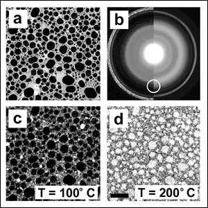
Fig. 1
To perform electron thermal microscopy, a system with unknown thermal characteristics is placed on the other side of the silicon nitride membrane. The membrane with metal islands on one side and an electrically active device is then inserted into the TEM with a different stage, custom built by the Cumings Group at the University of Maryland, for in situ voltage biasing. By applying power to the active devices, nanoscale thermal gradients can be produced and characterized by the metal islands. To demonstrate and calibrate the technique, the initial system chosen for study is palladium "heater wires", fabricated in the FabLab using standard electron beam lithography. A schematic of the wires and islands is seen in Fig. 2a, in perspective, top and side views. A bright field image of an actual device is seen in Fig. 2b. Again, voltage biasing the wires creates Joule heating which then produces local temperature gradients on the nanoscale (~10K/µm). Using the dark-field imaging outlined in Fig. 1, a map can be assembled in which the voltage required to melt an island is represented by color, seen in part c).
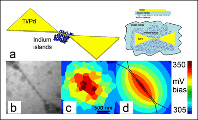
Fig. 2
Figure 2d depicts modeling of the device using finite-element analysis with colors taking the same meaning as in Fig. 2c. In our model, temperature is given by:
∇ · (K∇T) +Power = 0
(1)
where K is the local thermal conductivity, T is the temperature, and Power is given by
Power = σ|∇V|2.
(2)
Here, V is the electric potential, and σ is the electrical conductivity. The temperature dependence of σ is given by:
σ = σ0 (1 + α ΔT)-1
(3)
where σ0 is the room temperature value and α is the temperature coefficient of resistivity. Potential and conductivity are governed by the steady-state equation:
∇ · (σ · ∇V) = 0.
(4)
To test the model we leave thermal conductivity of silicon nitride as a free parameter. The lowest voltage needed to initiate melting matches the experimental value when we set the modeled thermal conductivity of silicon nitride to be 3.6 +0.5 -0.1 W/m·K.(The asymmetric uncertainty stems from melting point suppression.) This value is then used to produce the thermal map shown in Fig. 2d.
With measurements and modeling for a known system completed, the "heater wire" can be replaced with an unknown material, nanotubes and nanowires being suitable initial candidate materials. These devices can be thermally characterized during electrical operation, this is a natural advantage to the technique as so many nanomaterials are proposed as elements to complement existing electronic device architectures. The heater wire can also be left in position, with passive nanomaterials placed in the vicinity to see how their presence affects the resulting thermal maps.
Top